Semiconductor
Case 1: Precision PCB maintenance station project
Demand

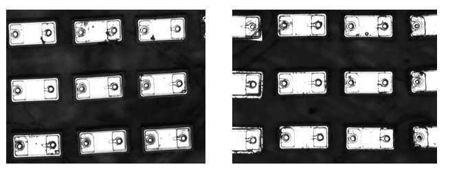
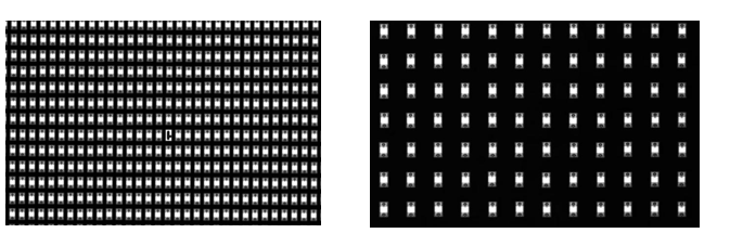
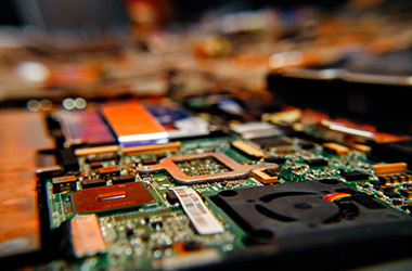
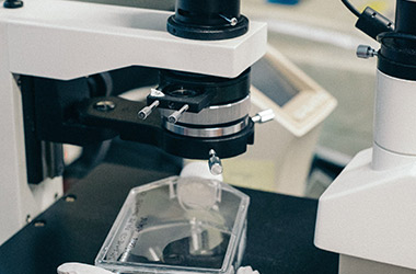
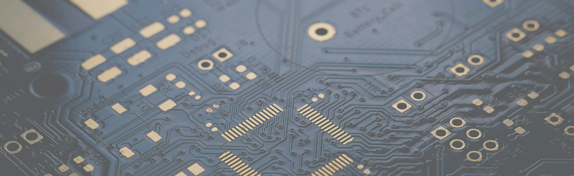
The precision PCB maintenance station is a workstation dedicated to the inspection and repair of precision circuit boards (PCBs) by professional operators using various tools and equipment to diagnose, repair, and test issues on the boards. The station is typically equipped with advanced instruments and equipment to support high-precision and efficient maintenance work.

Customer requirements for this project are:
1. Multiple base materials with BT < 5um damage/7um;
2. The base material has unique characteristics that make it difficult to achieve satisfactory inspection results using standard lighting;
3. Customized UV+3 color light detection is required, with a request for increased UV lamp power;
4. 10X/20X objective lenses.

Scheme Selection

Lens: Self-developed +6.5X electric zoom lens
Light source: MV-I8C-E-RGUV-G3
Others: MPD-5S-12C

Detection Effect

Case 2: MiniLED testing project
Demand

Mini LED detection uses COB (Chip on Board) technology, which involves packaging multiple chips on the same substrate. COB positioning for Mini LED detection is typically achieved through edge positioning, specific marker point positioning, alignment template positioning, and optical recognition technology. These methods can be used individually or in combination to ensure accurate detection and measurement of Mini LED. Using Muteng optical lenses for positioning during detection and measurement, the appropriate lens focal length and magnification can be selected based on specific requirements to obtain clear images and precise measurement results.

Customer requirements for this project are:
1. Flying inspection station: The product size (0.076-1.016) requires clear visibility of the polarity position of each individual chip for better positioning and mounting of the chips onto the backlight board.
2. Existing solution provider (Matech) uses a combination of MF100 tube len

Scheme Selection

Lens: MT-4.0-40C-NA013
Light source: MQ0428C-MV-IR

Detection Effect

Case 3: Separating machine project
Demand

The semiconductor automatic test and sorting machine is a high-end equipment in the field of numerical control, used for testing and sorting related devices in the semiconductor industry. It includes functions such as electrical performance testing, visual inspection, character marking, tape inspection, and automatic rewinding. Equipped with high-quality optical lenses, it can be used for image acquisition and analysis, precise positioning and alignment, optical parameter testing, defect detection and sorting, etc. It can detect and identify defects and surface problems on the devices, ensuring that the product quality and performance meet the requirements.

Customer requirements for this project are:
1.Consideration of the uniformity of light source illumination;
2.Consideration of the consistency of mass production of light sources;
3.Consideration of the contrast of imaging;
4.Limited installation space, production according to the customer's given size and st

Scheme Selection

Lens: MT1.5-110-HR
Light source: ML-C1716-W / ML-B62X14.5L / ML-B62X14.5R

Detection Effect

MORE CASE